
Case Study
Advances in Photoelectron Holography Pave the Way to Better Diamond-based Semiconductors
Novel 3D imaging technique enables scientists to observe the atomic arrangement of defects at the interface between diamond and metal oxides
Diamond could soon become an essential material for next-generation semiconductor devices. However, it is difficult to analyze the defects that form at the interface between diamond and other materials. To address this issue, scientists from Taiwan and Japan have developed a novel technique that can be used to image the 3D atomic arrangement at the interface of crystals and amorphous materials, shedding light about the nature and origin of defects.
The days when diamonds were prized only for their value as gemstones are long behind us. In addition to its well-established uses in polishing, cutting, and machining tools, diamond has been heralded for its use in semiconductor devices. Because of its remarkable carrier mobility, wide band gap, and thermal conductivity and stability, diamond could one day replace silicon—which, currently, is one of the mostly commonly used semiconductor materials—in high-performance electronic devices.
In recent years, scientists have come up with a way to use diamond as part of metal–oxide–semiconductor field effect transistors (MOS-FETs), which are a cornerstone component of modern electronics. The strategy in question requires an atomically thin layer of hydrogen atoms acting as an insulator between a diamond layer and an oxide layer; the more uniform and defect-free this layer, the higher the performance of the final device. In practice, this insulating layer is not perfect, as defects at the interface are common and difficult to control. However, understanding the causes and nature of these defects is challenging because we have no way of measuring their atomic arrangement without destroying the sample.
To address this issue, a research team including Professor Jun Mizuno from the Academy of Innovative Semiconductor and Sustainable Manufacturing at National Cheng Kung University (NCKU), Taiwan, is pioneering a new atomic imaging technique to peek at the interface between crystals and amorphous (non-crystalline) materials. It all started when Prof. Matsushita of Nara Institute of Science and Technology (NAIST) approached Prof. Mizuno to create a high-precision detection technique. The team’s novel approach, which resulted from a scientific research cooperation between Japan and Taiwan, was reported in Nano Letters and is based on photoelectron holography.
In simple terms, photoelectron holography involves shining a beam of light or high-energy electrons onto a sample and measuring the photoelectrons that are emitted as a result of this excitation. These photoelectrons are scattered by atoms in the immediate vicinity of the source before they move out, and this scattering effect is dependent on both, the angle of incidence of the initial beam and the precise arrangement of atoms and molecules in the target sample. Thus, by measuring the angle and energy of the photoelectrons, one can reconstruct a three-dimensional image of the sample’s atomic structure.
What the research team developed is an electron energy analyzer that helps measure the angular distribution of photoelectrons more efficiently. “Our analyzer is composed of three concentric spherical grids. When the second spherical grid is subjected to a voltage, photoelectrons with energies below this voltage are bounced back, whereas photoelectrons with energies higher than the voltage are projected forward onto a screen,” explains Mizuno, “This device therefore acts as a high-pass energy filter of photoelectrons and enables us to detect weak signals coming from defects at the interface.” Fabricating these novel spherical grids required a combination of 3D nano- and micro-fabrication, plating, and thin-film deposition technologies.
Using this analyzer, the researchers captured photoelectron holograms from different diamond-based MOS-FETs at the diamond–aluminum oxide interface with unprecedented precision. This enabled them to reconstruct the possible 3D atomic arrangements at the interface and correlate these findings with the measured electronic performance of the devices. To further verify their findings, the team also conducted theoretical simulations of photoelectron holograms of atomic interfaces and compared them with the experimental data.
Such a spherical grid has never been realized before. This could be key to expanding the frontiers of semiconductor materials, a goal which the NCKU’s Academy of Innovative Semiconductor and Sustainable Manufacturing is constantly working towards achieving. “We are convinced that our work will become an important evaluation technology for the development of cutting-edge semiconductor devices,” remarks Mizuno, “Our study has already confirmed that our technique is particularly useful to analyze diamond-based devices, which will become more important in the future.”
Let us hope this novel evaluation method helps us bridge the gap to develop next-generation semiconductors!
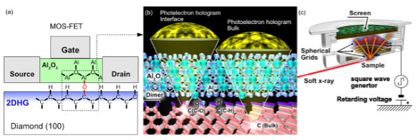
Image / Novel photoelectron holography technique lets us reconstruct 3D atomic arrangements at crystal/amorphous material interfaces.
Reference
AuthorsMami N. Fujii1,2, Masaki Tanaka2, Takumi Tsuno2, Yusuke Hashimoto2, Hiroto Tomita2, Soichiro Takeuchi2, Shunjo Koga2, Zexu Sun2, John Isaac Enriquez3, Yoshitada Morikawa3, Jun Mizuno4,5, Mutsunori Uenuma2, Yukiharu Uraoka2, and Tomohiro Matsushita2
Atomic Imaging of Interface Defects in an Insulating Film on Diamond
Nano Letters
Affiliations
1Faculty of Science and Engineering, Kindai University
2Graduate School of Science and Technology, Nara Institute of Science and Technology
3Department of Precision Engineering, Graduate School of Engineering, Osaka University
4Research Organization for Nano and Life Innovation, Waseda University
5Academy of Innovative Semiconductor and Sustainable Manufacturing, National Cheng Kung University (NCKU)
Professor Jun Mizuno received a PhD degree in Applied Physics from Tohoku University, Japan, in 2000. He is currently a Professor at NCKU’s Academy of Innovative Semiconductor and Sustainable Manufacturing. His research interests lie in device science, including the development of micro-components for MEMS, surface science, numerical simulations, and the development of flexible components, electronic packaging, and advanced medical components. He has over 110 publications to his name on these topics.
Partner Institutions